Project Name | Microelectronics Agenda (PRR)
Main objective | Increase the competitiveness and resilience of the economy based on R&D, innovation, diversification and specialisation of the productive structure
Leading Entity | ATEP - AMKOR TECHNOLOGY PORTUGAL, S.A
Eligible investment (AGENDA) | 67,5 million €
Eligible investment (PICADVANCED) | 4,2 million €
Start Date | 2022-01-01
End Date | 2024-12-31
The Microelectronics Agenda has been drawn up in an integrated manner and in line with the European initiative in the area of microelectronics, with the main objective of solving the challenges facing this industry, with the aim of unlocking the full potential of the microelectronics area and adding value to European society. This will be achieved through a series of scientific and technological investments by the various organisations, aimed at strengthening the production and innovation capacity of the national semiconductor industry. In line with Europe's need to respond to the shortcomings of the global semiconductor market, this national agenda aims to:
- Training the sector's organisations in the trends/challenges of this technological market, through strategic productive investments and the development of new technologies, processes and systems;
- Further digitise the sector by investing in Industry 4.0 technologies and contributing to the growth of new communication technologies;
- Promote coordination between research centres, companies and other entities in order to bring together the necessary skills and level of innovation;
- Investing in greater sustainability in a sector that consumes a lot of raw materials and precursors, in order to reduce its ecological footprint;
- Investing in qualifications in key skills that stimulate growth and competitiveness, increasing the level of qualification and specialisation in the area of microelectronics and creating qualified employment, alleviating the social and economic crisis;
- Contribute to a more cohesive, competitive and prepared Europe in the sector.
More specifically, PICadvanced's main objective is to intervene in the WP2 and WP13 (lead) sub-projects, which aim to:
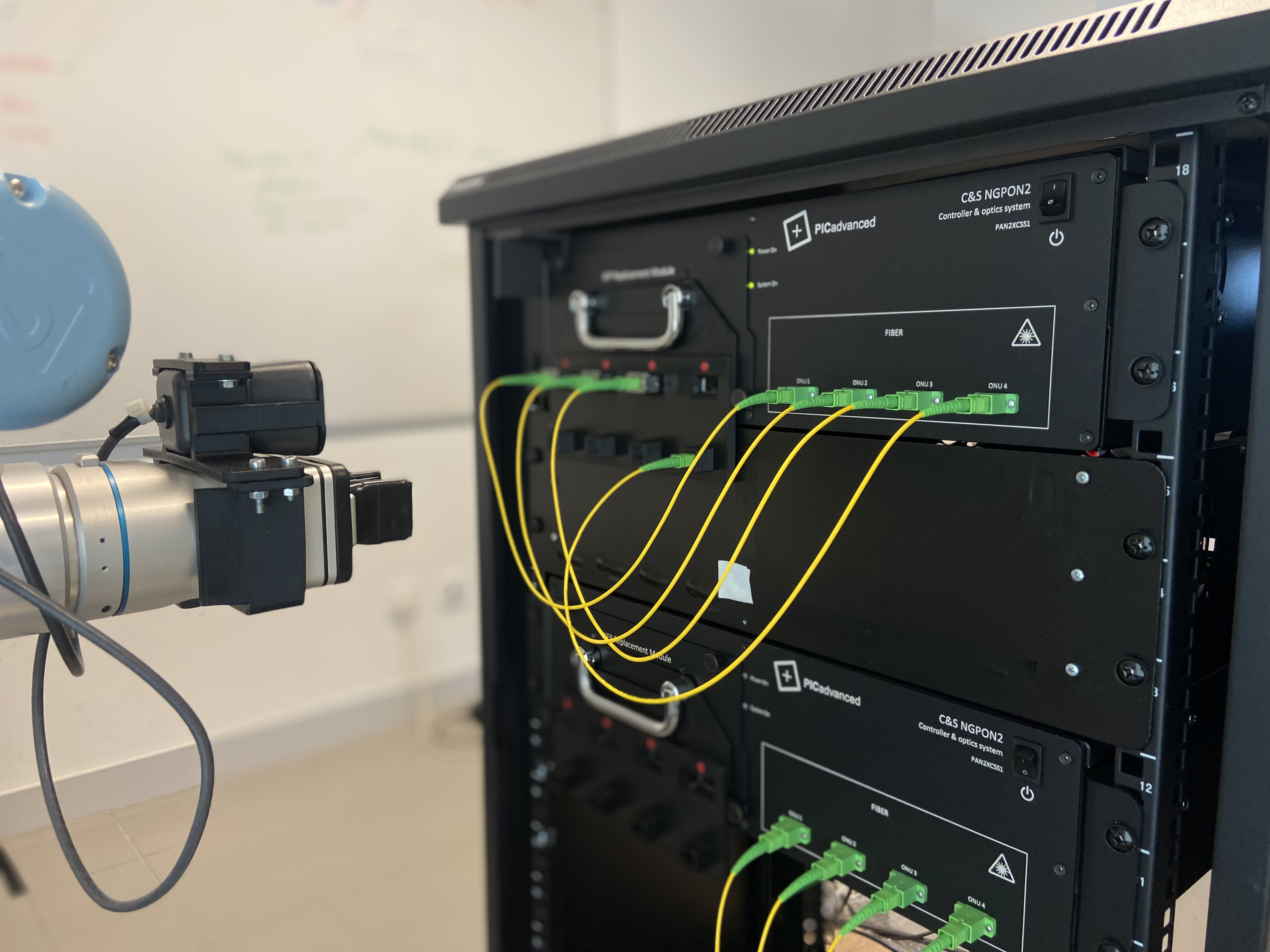
- Development of photonic integrated circuits (PICs) for future telecoms networks - specifically 25G and 50G networks and 5G/6G radio networks.
- Industrial encapsulation and industrialisation processes for optical transceivers with a view to robotic line integration
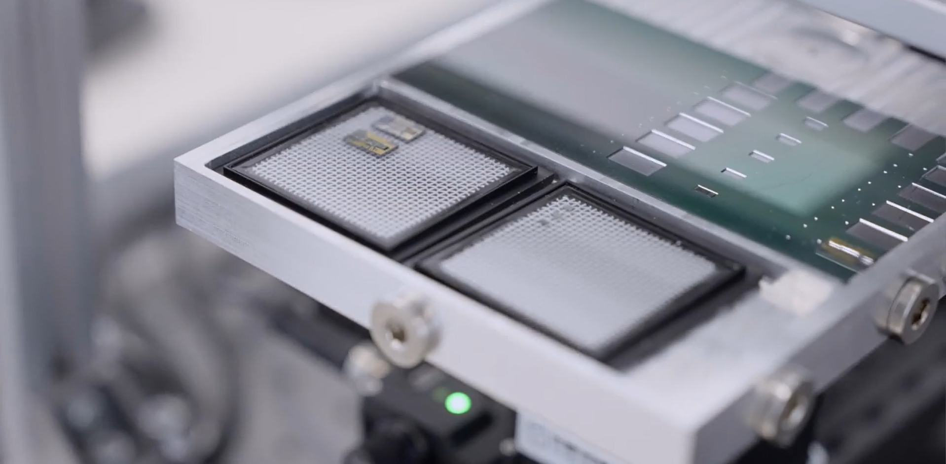
- Industrial processes for encapsulating integrated optical circuits, with the development of equipment and tools for encapsulating integrated optical circuits
- Training and testing of processes for large-scale production of microfabricated structures for packaging integrated optical circuits.


